15: (5,0) Carbon Nanotube — Transport properties
Note that these systems require reasonably large-scale electronic structure calculations.
Bulk Transport properties
-
Outline: Obtain the quantum conductance of a pristine single-walled carbon nanotube
-
Directory:
tutorials/tutorial14/periodicFiles can be downloaded from here -
Input Files
-
cnt.scfThepwscfinput file for ground state calculation -
cnt.nscfThepwscfinput file to obtain Bloch states for the conduction states -
cnt.pw2wanInput file forpw2wannier90 -
cnt.winThewannier90input file
-
First we consider a single unit cell, with 10 k-points. With
transport_mode = bulk we compute the transport properties of a
pristine, infinite, periodic (5,0) carbon nanotube. Later, we will
compare the quantum conductance of this system with a defected nanotube.
-
Run
pwscfandwannier90. -
The quantum conductance and density of states are written to the files
cnt_qc.datandcnt_dos.dat, respectively.
LCR transport properties — Defected nanotube
-
Outline: Use the automated LCR routine to investigate the effect of a single silicon atom in a infinite (5,0) carbon nanotube.
-
Directory:
tutorials/tutorial15/defectedFiles can be downloaded from here -
Input Files
-
cnt+si.scfThepwscfinput file for ground state calculation -
cnt+si.nscfThepwscfinput file to obtain Bloch states for the conduction states -
cnt+si.pw2wanInput file forpw2wannier90 -
cnt+si.winThewannier90input file
-
In this calculation an 11-atom supercell is used with a single silicon substitutional defect in the central unit cell. The supercell is chosen so that is conforms to the 2c2 geometry (see User Guide for details) with principal layers set to be two unit cells long.
-
Run
pwscfandwannier90. Again these are large calculations, progress can be monitored by viewing respective output files. -
The quantum conductance is written to
cnt+si_qc.dat. Compare the quantum conductance with the periodic (bulk) calculation. Your plot should look like this{reference-type="ref" reference="fig:cnt_qc"}.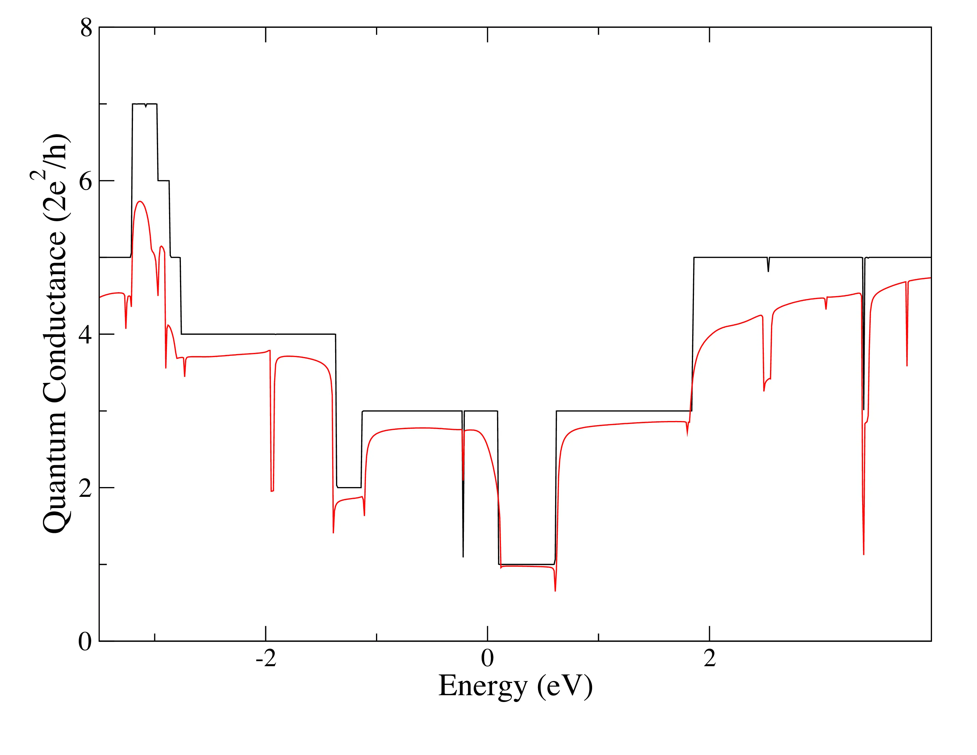
Quantum conductance of infinite pristine nanotube (black) compared to that of the infinite nanotube with the substitutional silicon defect (red).
Further ideas
-
Set
write_hr = truein the bulk case. Consider the magnitude of Hamiltonian elements between Wannier functions in increasingly distant unit cells. Are two unit cell principal layers really large enough, or are significant errors introduced? -
Does one unit cell either side of the defected unit cell shield the disorder so that the leads are ideal? Does the quantum conductance change if these 'buffer' regions are increased?